
Applied Materials and Besi expand packaging tie-up at $5bn EPIC Centre
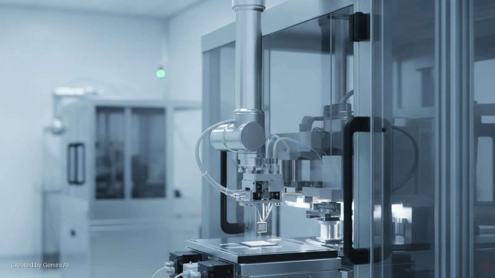
Applied Materials (NASDAQ: AMAT) and BE Semiconductor Industries (Besi, Euronext Amsterdam: BESI) have expanded their strategic partnership, with the Dutch assembly-equipment maker joining Applied's newly built EPIC (Equipment and Process Innovation and Commercialisation) Center in Silicon Valley as an Innovation Partner. The move deepens a collaboration that dates to 2020, when the two companies established a joint Hybrid Bonding Centre of Excellence at Applied's Advanced Packaging Development Center in Singapore.
That six-year partnership produced Kinex, a die-to-wafer hybrid bonding system that Applied describes as the first integrated product of its type. The new arrangement extends joint R&D beyond hybrid bonding into thermo-compression bonding (TCB) scaling, die-on-wafer, die-on-die and die-on-panel integration platforms, and photonics-enabled interconnect applications for co-packaged optics.
The expanded scope
Under the Innovation Partner arrangement, Besi engineers will be embedded alongside Applied's teams at the EPIC Center, working on a unified development flow that treats advanced packaging as a front-end materials engineering discipline rather than a back-end assembly step. Applied's Dr. Prabu Raja, president of the Semiconductor Products Group, framed the rationale directly: "Developing these technologies together with Besi engineers in a front-end R&D environment like the EPIC Center will allow us to treat them as one connected flow rather than a series of isolated steps."
The four R&D programmes named in the announcement target next-generation 3D IC scaling for AI compute and memory, new hybrid bonding platforms building on the Singapore centre, TCB process ecosystem development, and photonics interconnect work supporting co-packaged optics.
Applied's EPIC Center carries a capital commitment expected to reach approximately $5 billion as customer projects scale up. The facility is described as operationally ready in 2026 and is positioned by the company as the largest single US investment in semiconductor equipment and process R&D.
Market context
The partnership reflects a structural shift under way across the semiconductor supply chain. AI workloads are exhausting the performance gains available from classical transistor scaling, pushing chipmakers toward heterogeneous integration: stacking logic, memory and I/O dies in densely interconnected packages rather than shrinking them on a single monolithic die. TSMC's CoWoS and SoIC platforms, Intel's Foveros, and Samsung's X-Cube are all competing to serve this demand, with advanced packaging capacity now as strategically constrained as leading-edge wafer fab nodes.
That dynamic has elevated the commercial importance of assembly-equipment suppliers such as Besi, which historically occupied a lower-margin segment of the value chain. Tight coupling between equipment vendors and process specialists is increasingly where differentiation is won, as the line between wafer fabrication and packaging dissolves. Co-locating Besi engineers inside Applied's flagship R&D centre is a direct response to that convergence.
Competitive and regulatory read-across
The tie-up also carries export-control relevance. Both companies have significant customer exposure in Asia Pacific, and advanced packaging technology has attracted growing scrutiny from US export regulators alongside front-end chip-making equipment. The US Bureau of Industry and Security has progressively tightened controls on semiconductor manufacturing equipment destined for certain markets, and advanced packaging is widely expected to come under closer review as its strategic importance grows. Neither company addressed this dimension in the release.
For AI infrastructure buyers and hyperscalers investing in next-generation accelerators, the near-term signal is that co-optimised packaging solutions from the Applied-Besi pipeline could reach high-volume manufacturing faster than through sequential development. The partnership's first measurable milestone will be whether joint programmes at the EPIC Center yield commercially available TCB or hybrid bonding tools ahead of competing roadmaps from rival equipment consortia.