
Applied Materials opens $5bn EPIC Centre for chip R&D in Silicon Valley
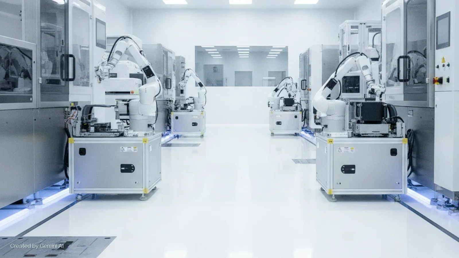
Applied Materials has officially opened its Equipment and Process Innovation and Commercialisation (EPIC) Centre in Sunnyvale, California, a facility the company describes as the largest of its kind dedicated to collaborative semiconductor process technology and equipment research. The capital investment is expected to reach approximately $5 billion as customer projects scale up over time.
The 600,000-square-foot building houses close to four acres of advanced cleanroom space and took more than six million construction hours to complete. Applied says the facility is designed to collapse the traditional, sequential R&D pipeline, in which materials research, equipment development and process integration have historically occurred in separate environments with formal handoffs between each stage. At EPIC, those activities will run in parallel, with partner engineers embedded on site alongside Applied's own scientists.
Partners and scope
The founding partner roster spans the principal nodes of the global chip supply chain. Logic and memory manufacturers TSMC, Intel, Samsung Electronics, Micron and SK hynix have committed to work inside the facility. They are joined by innovation partners Broadcom, Advantest, SCREEN Holdings, KIOXIA and BE Semiconductor (Besi), as well as five US research universities: Arizona State University, Rensselaer Polytechnic Institute, Stanford University, UC Berkeley and UCLA Samueli School of Engineering.
Gary Dickerson, president and chief executive of Applied Materials, said the complexity of AI-era chipmaking had made the traditional single-company R&D model insufficient. "To win the race for AI leadership, our industry must rethink and re-engineer how we collaborate to develop and commercialise the next generation of semiconductor technologies," he said.
TSMC chairman and chief executive C.C. Wei noted that leading-edge production nodes have shrunk from 350 nanometres to 2 nanometres over the past three decades, a 175-fold reduction in feature size, and argued that continued scaling will require ever-closer equipment and foundry collaboration. Intel chief executive Lip-Bu Tan said his company sees a path to more than one trillion transistors in a single package by 2030, a target that makes tighter equipment partnership commercially essential.
Market and competitive context
Applied Materials already holds dominant positions in chemical mechanical planarisation, physical vapour deposition and several etch categories, and the EPIC Centre consolidates that leverage by giving it sight lines across multiple customer roadmaps simultaneously. Rivals Lam Research and Tokyo Electron operate their own customer-collaboration programmes, but Applied's investment scale and the breadth of its founding partner list set a high bar for comparable industry coalitions.
The centre arrives at a moment when AI-driven demand for advanced logic and high-bandwidth memory is accelerating capital expenditure across the semiconductor industry, while geopolitical pressures are pushing chipmakers to diversify and de-risk their technology development pipelines. EPIC is sited entirely in the United States, which aligns with the objectives of the CHIPS and Science Act, though Applied did not cite federal funding in its announcement and has not confirmed whether any CHIPS programme incentives are attached to the investment.
University partnerships with Arizona State, Stanford, UC Berkeley, RPI and UCLA also position EPIC as a talent pipeline mechanism, an increasingly competitive priority as the industry faces a well-documented shortage of semiconductor process engineers. The facility's scale, the seniority of its founding partners, and the depth of university engagement suggest it will become a meaningful proving ground for advanced packaging, 3D integration and materials innovation over the next decade.