
GlobalFoundries to operate two new New York fabs in $21bn US-Japan deal
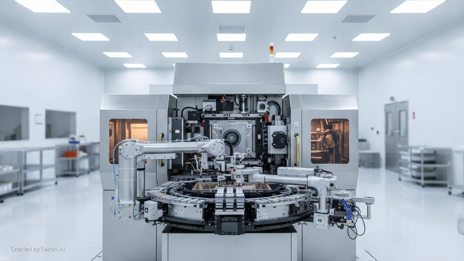
GlobalFoundries (GFS) has been selected as technology provider and operator for two new semiconductor fabrication facilities at its existing Malta, New York, site, under a US-Japan initiative that carries up to $21 billion in funding. The agreement, enabled by a bilateral trade and investment deal brokered by the Trump administration, represents one of the largest single commitments to domestic semiconductor manufacturing since the CHIPS and Science Act came into force.
Japan will provide the capital. GlobalFoundries will contribute its process technology, manufacturing expertise and operational infrastructure. An initial $10 billion tranche will fund the first 300mm fab, which the company expects to be operational by 2029. A second $10 billion investment, described as conditional, would fund a matching facility. At full run-rate, each fab is projected to add approximately 900,000 300mm wafer starts per year to US capacity.
"This is a bold new initiative for semiconductor manufacturing, bringing together the United States and Japan with GF's differentiated technology and decades of manufacturing expertise to accelerate trusted capacity in New York," said Tim Breen, chief executive of GlobalFoundries. The company expects to break ground on the first fab before the end of this year, with the Malta site described as permitted and shovel-ready.
Customer and government backing
The release is notable for the depth of named customer endorsements it carries. Apple chief operating officer Sabih Khan linked the deal explicitly to Apple's $600 billion US investment commitment and described GlobalFoundries as an inaugural member of the company's American Manufacturing Programme. Renesas chief executive Hidetoshi Shibata said Renesas is planning around the new New York capacity as an extension of its own production footprint. General Motors president Mark Reuss cited the expansion as supporting GM's semiconductor supply agreement with GlobalFoundries, the first direct automaker-to-foundry deal of its kind. Cirrus Logic also confirmed it sees the new fabs as a source of domestic mixed-signal production capacity.
In a separate but related agreement, GlobalFoundries and the US Department of Commerce have amended the company's existing CHIPS Act award to reallocate $955 million toward silicon photonics, silicon-germanium and advanced packaging programmes at its Malta and Burlington, Vermont, sites. The Department of Commerce will also take an approximately four percent equity stake in GlobalFoundries, giving the federal government a direct financial interest in the company's performance.
The project is expected to generate around 27,000 construction and ecosystem jobs and more than 1,000 permanent high-skilled manufacturing roles in New York's Capital Region.
Market and geopolitical context
The announcement arrives at a moment of acute focus on semiconductor supply-chain resilience among Western governments. The US CHIPS Act, enacted in 2022, allocated $52 billion for domestic semiconductor investment, and the GlobalFoundries award is among the larger single-site commitments to flow from that framework. The US-Japan alignment on semiconductor policy has been building since the two governments agreed to coordinate on critical technology supply chains; Japan has separately invested in domestic capacity through the Rapidus project and has supported TSMC's Kumamoto fab expansion.
GlobalFoundries occupies a distinct position in this landscape. Unlike TSMC or Samsung, it does not pursue leading-edge logic below roughly 12nm; instead, it focuses on differentiated process technologies including RF, embedded non-volatile memory, and silicon photonics, which are critical for automotive, industrial and connectivity applications rather than high-volume consumer compute. The emphasis on 300mm wafers for automotive and connected-infrastructure markets reflects a deliberate positioning away from the AI-accelerator race, where TSMC and Samsung dominate advanced-node volume.
The 2029 timeline for the first fab to come online is realistic but exposed to construction risk. TSMC's Arizona expansion has experienced well-documented schedule slippage attributable to skilled-labour shortages and supply-chain constraints, and GlobalFoundries will need to demonstrate it can avoid similar delays. Investors will watch the groundbreaking later this year and subsequent construction milestones as early proof points.